a) EDS spectrum under TEM of a single Bi 2 Se 3 nanoplate. (b) EDS
a) EDS spectrum under TEM of a single Bi 2 Se 3 nanoplate. (b) EDS

SEM-EDS Information Depth - The XPS Library of Monochromatic XPS Spectra
Facile synthesis of Bi 2 Se 3 /nitrogen-doped carbon dot nanoplates for aqueous zinc ion battery cathodes - Physical Chemistry Chemical Physics (RSC Publishing) DOI:10.1039/D3CP02669H

Thermoelectric effect and devices on IVA and VA Xenes - Zhu - 2021 - InfoMat - Wiley Online Library

Oriented Attachment of 2D Nanosheets: The Case of Few-Layer Bi2Se3

a) Field emission scanning electron microscopy (FESEM) images of Bi 2
Optical transmission enhacement through chemically tuned two-dimensional bismuth chalcogenide nanoplates

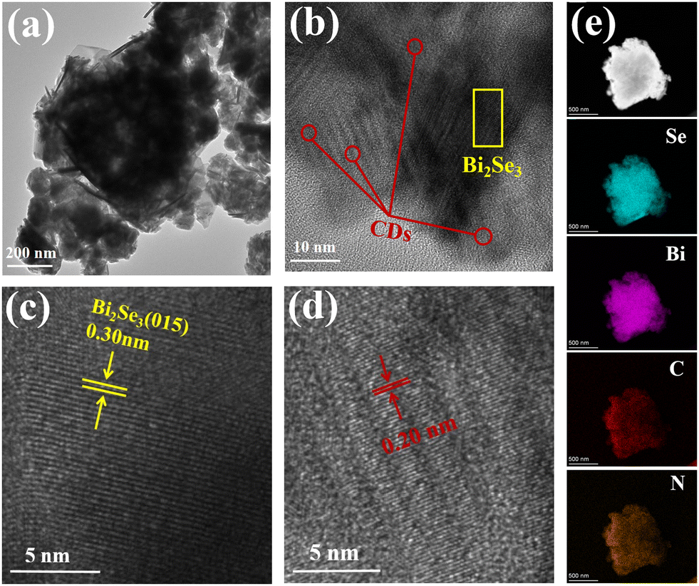
TEM and EDS characterizations. (a, b) TEM images of a typical Bi2Se3

a-d) TEM images of different Bi2Se3 nanostructures. The insets show
Chemical Characterization of Nanowires

One‐dimensional and two‐dimensional synergized nanostructures for high‐performing energy storage and conversion - Li - 2020 - InfoMat - Wiley Online Library


